
A Quad Flat No-Lead package is a surface-mount semiconductor package that has electrical contacts (pads) on the bottom surface instead of protruding leads. It provides a compact footprint, excellent electrical performance, and efficient thermal dissipation through an exposed thermal pad.
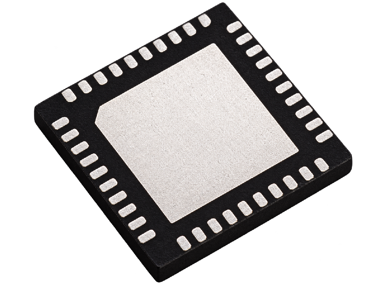

Low electrical parasitics for high-speed applications Compact and lightweight design

Suitable for high-frequency and high-power applications Excellent thermal dissipation (exposed thermal pad)

Wettable flank option for easy solder joint inspection (AOI)
Parameter
Specification
Package Size
1x1 mm to 13x13 mm
Die Size
0.5x0.5 mm to 10x10 mm
Wire Diameter
0.6 mil - 1.3 mil
Wafer Thickness
>100 µm
Leadframe Thickness
100-300 µm
Package Thickness
0.50 mm to 1.45 mm